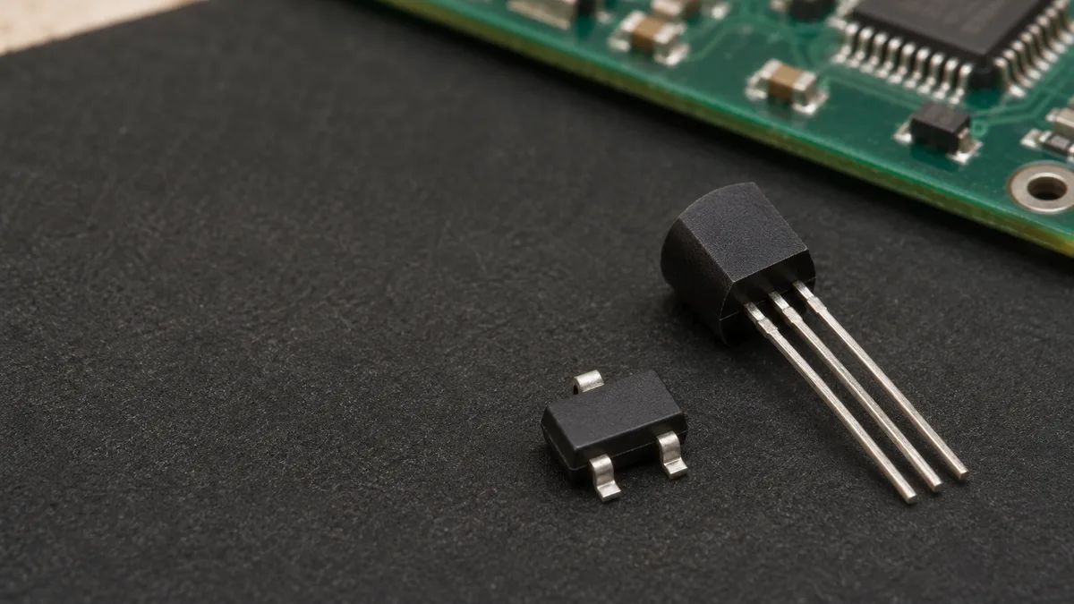
MMBT3904 and 2N3904 are both NPN transistors with matching 40 V and 200 mA headline ratings, but they are not interchangeable on a PCB. The MMBT3904 uses a SOT-23 surface-mount package, while the 2N3904 uses a TO-92 through-hole package. Beyond the physical layout, their pin numbering for the base and emitter is reversed, and their listed thermal ratings differ. You must compare the exact drawings, test conditions, and circuit requirements before approving a substitution.
The Datasheet Versions Define the Scope
This comparison uses two specific MCC documents:
MCC MMBT3904 datasheet, Rev.3-6-08182023
MCC 2N3904 datasheet, Rev.3-2-12012020
All page references below point to these revisions. Do not extend these conclusions to another manufacturer's version without checking their own data.
The StockWake MMBT3904 listing names Micro Commercial Components (MCC). That manufacturer reference supports using MCC documents here. But it does not identify every ordering suffix, nor does it verify a particular offered lot against the drawings. Keep the full ordering code separate from the base device name. Both datasheets have ordering information on page 4.
The Packages Use Different Mounting Styles
The SOT-23 drawing shows a surface-mount package with short terminals. The TO-92 drawing shows a body with leads for through-hole mounting. These are different physical layouts. A board designed for one cannot be treated as accepting the other simply because the transistor names both end in "3904".
Pin Functions Need a Numbered Map
The Base and Emitter Use Different Numbers
The MCC terminal legends assign different numbers to the base and emitter.
MMBT3904: Base is pin 1, emitter is pin 2.
MCC 2N3904: The numbered roles are reversed. Emitter is pin 1, base is pin 2.
Collector is pin 3 in both documents. Match each circuit connection to its function, rather than carrying the same pin number across the comparison.
The Original Drawing Keeps the Position Clear
Use the numbered package drawing on page 1 of each linked MCC datasheet. The terminal roles in the table below follow those source legends. Neither page explicitly labels the drawing as "Top View" or "Bottom View". Keep the source drawing and pin numbers together when checking a PCB footprint. Do not infer physical orientation from a left-to-right description alone.
Package and Numbered Terminal Comparison
Comparison Point | MCC MMBT3904 | MCC 2N3904 |
|---|---|---|
Document revision | Rev.3-6-08182023 | Rev.3-2-12012020 |
Package and mounting | SOT-23; surface mount | TO-92; through hole |
Base | Pin 1 | Pin 2 |
Emitter | Pin 2 | Pin 1 |
Collector | Pin 3 | Pin 3 |
Drawing reference | Page 1 numbered outline and internal structure | Page 1 numbered outline and terminal legend |
A body marking is another identification field. The guide to top markings and complete part numbers explains that distinction. A marking alone should not replace the manufacturer and ordering code used for this comparison.
Thermal Ratings Need Their Reference Conditions
The Listed Dissipation and Thermal Resistance Differ
MCC lists 350 mW for the MMBT3904 and 625 mW for the 2N3904. Their junction-to-ambient thermal resistances are 357°C/W and 200°C/W, respectively. The documents do not establish a shared test board for these ratings. The MMBT3904 also lists a junction-to-case value of 185°C/W. Do not compare that value with the 2N3904's junction-to-ambient figure as though they describe the same heat path.
Ambient Derating Does Not Define the Same PCB
Both page 3 derating curves use ambient temperature on the horizontal axis. Each is flat from 0°C to 25°C, then falls to zero at 150°C. At that endpoint, the plotted allowable dissipation is zero. It does not show powered operation at 150°C ambient. The datasheets separately list a maximum junction temperature of 150°C.
The inspected documents do not specify the board material, copper area, or airflow behind the thermal figures. Their listed dissipation ratio therefore cannot establish the ratio of allowable device dissipation in your assembly. Keep those missing conditions visible rather than assigning both parts an invented common test board.
Electrical Conditions Complete the Circuit Comparison
Matched Test Points Reveal Electrical Differences
The headline voltage and current ratings match, but not every electrical specification does. At 50 mA collector current and 5 mA base current, the maximum collector-emitter saturation voltages differ. For transition frequency, the test conditions match between the two datasheets, but the minimum values differ. Keep the minimum or maximum designation beside each value.
Electrical and Thermal Values With Their Conditions
Parameter and Basis | MCC MMBT3904 | MCC 2N3904 | Condition and Source Page |
|---|---|---|---|
VCEO rating | 40 V | 40 V | Page 1 maximum ratings at 25°C unless specified |
IC rating | 200 mA | 200 mA, labelled continuous | Page 1 maximum ratings |
Listed dissipation | 350 mW | 625 mW | Page 1 ratings at 25°C unless specified; page 3 Fig. 6 ambient derating |
Junction-to-ambient resistance | 357°C/W | 200°C/W | Page 1; detailed board conditions not stated |
VCE(sat) maximum | 0.3 V | 0.4 V | 25°C; IC = 50 mA; IB = 5 mA; page 2 |
fT minimum | 300 MHz | 250 MHz | 25°C; VCE = 20 V; IC = 10 mA; f = 100 MHz; page 2 |
hFE minimum–maximum* | 100–300 | 100–300 | 25°C; VCE = 1 V; IC = 10 mA; pulse width ≤300 µs; duty cycle ≤2.0%; page 2 |
Both page 2 tables use 25°C unless otherwise specified. An asterisk marks the collector-emitter breakdown voltage and DC current gain entries. Its footnote specifies pulse width ≤300 µs and duty cycle ≤2.0%. The VCE(sat) rows are not starred; this comparison does not assign that footnote to them or infer an unstated continuous-test duration. Do not use hFE at VCE = 1 V as a guarantee of saturation at another operating point. The 100 MHz entry is the stated measurement frequency for fT, not a second transition-frequency limit. Likewise, fT is not a guaranteed circuit switching frequency.
The Operating Point and PCB Set the Change Boundary
The practical question is whether the proposed device meets the actual mounting, connection, and operating requirements. Compare the relevant current, base drive, voltage, and thermal conditions with the data. Shared maximum ratings do not establish acceptable operation under every combination of those conditions.
If the technical review later approves an alternative, the guide to recording an approved alternative covers preserving that decision. This datasheet comparison does not supply the approval or validate an actual PCB.
Frequently Asked Questions
1. Are MMBT3904 and 2N3904 the same transistor in different packages?
The reviewed MCC versions share NPN polarity and some headline ratings. They differ in package, numbered terminal roles, thermal ratings, and some electrical specifications. Describing the difference as packaging alone leaves out relevant information.
2. Which MCC pin numbers identify the base and emitter?
For the MCC MMBT3904, base is pin 1 and emitter is pin 2. For the reviewed MCC 2N3904, emitter is pin 1 and base is pin 2. Read these numbers with the original drawings, not an unqualified left-to-right rule.
3. Does the TO-92 rating guarantee higher allowable dissipation on my board?
Not by itself. It is a higher listed dissipation rating. It does not establish how much power either device can dissipate in your actual assembly. The documents do not give a common board and airflow basis. Check the applicable ambient derating and mounting conditions.
4. Can the two packages use the same PCB footprint?
Not directly. Their package layouts and mounting styles differ. Any different mounting arrangement needs its own design assessment; this comparison does not validate one.
5. Which test conditions must stay with the electrical comparison?
Retain temperature, collector current, base current, or collector-emitter voltage as applicable, plus frequency and starred pulse conditions. Preserve whether each number is a minimum, maximum, or rating. A value without its test point can answer the wrong circuit question.
Start with the correct MCC revisions, preserve the numbered pin map, and compare thermal and electrical data on their stated basis. Then identify which differences affect the existing PCB and operating point. The useful result is a specific technical comparison with visible limits, rather than a blanket interchangeability claim.